S100 Computers

HomeS-100 Boards HistoryNew BoardsSoftwareBoards For Sale
ForumOther Web SitesNewsIndex  

A 16 MB Static S-100 RAM Board
This 16MB static RAM board has now gone through a number of improvements/versions.  It should be the only RAM board you will need in your S100 system since it contains 16MB of RAM (24 address lines), the full addressing capability of the S100 bus -- not counting our own "Overhead Bus Address lines" where one can address up to 4GB of RAM in theory.

The major versions of this board in the past were:-
     
V1   This was the original 16 MB RAM board.  It was modeled after the 4MB Static RAM board made and well tested earlier. This board utilized two small mezzanine RAM boards to house the actual eight RAM chips.
V3   This board eliminated the meazzanine board, had an 8MB or 16MB capacity with the RAM chips soldered directly to the board.
V5   This board eliminated many of the TTL 74LSxx  chips on the V3 board utilizing two 22V10 GAL's instead.  The board was faster and could accomidate the two mezzanine boards OR have the RAM chips could be soldered directly to the board.
V6   This board further simplified the board circuitry of the V3 and V5 boards. Bidirectional 74LS645 buffers are used to deliver 8 or 16 bit data to the S100 bus.  Wide critical signal traces were used. All minor errors on the previous boards have been corrected. 


 Final Production Board
  
16MB RAM V3
V6 Board
  V6 Board-2
     
Introduction, 

Our 4MG Static RAM board turned out to be a great success. Its 4M of static RAM could be located anywhere in the S100 buss's 16MB address space with four of these boards filling up the buss's total address space.   The board was fast and could handle 8 and 16 bit data paths 100% reliably with all the CPU's I could throw at it.  It reliably ran with our Z80, 6502, 8088, 8086, 80286, 68000 and our prototype 80386 CPU boards.  Neither have I found a vintage S100 CPU board that would not work with it.

As we start moving towards 32 bit CPU's RAM address space becomes a bigger issue for the types of programs these CPU's are typically used for.   It seemed to make sense to design a new RAM board that would incorporate a total of 16MB on one board.   It also seemed to make sense utilize the well established circuitry of our 4M static board. Essentially use a larger capacity RAM chip and shift all the address lines up two bits.

There is one problem however.  As best I can tell nobody makes a 2M X 8 static RAM chips in a DIP chip format.   In line with current trends,  all new  high capacity static RAM chips are in a surface mount format.    This for a long time put me off doing such a board.  Not only was the routing/layout of the board extremely complex, but with all chips nailed down on the board, prototypes and changes became expensive.   Andrew Lynch came up with the idea of utilizing a small mezzanine board with only 4 RAM chips and  its own pin/socket changed all that.  These mezzanine boards could be assembled separately and moved around from board to board.  I am already using them on our prototype 30386 32MB RAM board.  Here is a picture of such a mezzanine board:-
   
 V06c Mezzanine Board
    
We have designed these mezzanine boards such that they can be used not only in this board but also in larger RAM boards for the future 80386, 80486 etc.  See for example our prototype 32MG Static RAM board.

The actual static RAM chips we will use here are the Cypress 2MG X 8 (CY62167's).  They come in two formats, the CY62167E which runs with a Vcc voltage of 5 Volts and a CY6216DV30 which runs with a  Vcc of 3.5 Volts.  Both are available from a number of venders -- though there is a wide price range. The 5 Volt units are a little more expensive.  I get mine from Mouser (727-CY62167ELL-45ZXI).    They are not cheap ~$18 each.  So it will cost you about $144 in RAM chips to completely fill your S100 bus system with this board.  Not bad when you remember that once upon a time you paid that for 1K of RAM!  The board has a 5 volt and 3.5V regulator to accommodate both chips.  (Note in passing, by mistake once I actually jumpered the 3.5V RAM chips to the 5V supply. They ran fine before and afterwards -- though I don't recommend doing this).

Memory Board Logic
The RAM chip support logic on this board is almost identical to that of our 4M Static RAM board.   Before you go further you should familiarize yourself with how RAM data is processed on the S-100 bus using 8 and 16 bit CPU's.  This is described in some detail here.
 

A First Prototype 16 MG Static RAM Board
One thing that takes a little getting use to with a board of this capacity is the fact that there is actually no need for a board address selection circuit.   Any S100 bus RAM should in theory be contained on this board.   However there are times where one may wish to only use only part of the S100 busses address space.  For this reason two 74LS682's are utilized for RAM selection.  The S100 bus Phantom line is also factored in. The relevant circuit is shown here:-

 Board Selection


By far the most complicated section of the board is the 8/16 bit data selection circuit.   While it is crying out for a PAL chip, it is also easily implemented with a few fast 74Fxx chips.   That worked well with our 4M RAM board. We will use it again here.
    
  Pal Circuit2

Soldering Surface Mound RAM chips.
Soldering (expensive) surface mount chips is not for everybody. For many years I avoided using these chips not only because I felt they were difficult to solder but because once added to a board they cannot easily be removed.   Many of the prototype boards require a number of versions. Being able to swap chips is not only quick and easy but you know you have a reliable chip set.
 
However I have to say soldering these RAM chips to the mezzanine board was quite easy.  There are many discussions on the Web about SMT soldering.   I found this U-Tube video helpful.  It turned out to be far easier than expected.

The steps are:-

Use a very fine tip 10-15W soldering iron.  The tip must be small enough not to bridge two RAM chip pins.
With a small brush cover the board solder pads with solder paste (I use, DeoxIT Rosin Soldering Flux).
Then lightly add solder to all the board pads. You can more or less slobber/draw the tip down the pads quickly.
The solder past will not allow solder to reside between the pads.
Reflux all the pads
Carefully align pin one on the circuit board pad so the visible pad is equal on both sides of the chip. (i.e. the chip is exactly centered).
Touch pin 1 with the soldering iron. If it is clean no solder is required. There is sufficient solder on the board and chip to make a connection.
Next go to pin 25. Carefully align the chip so all pins are exactly over the circuit board pads.
Solder exactly as for pin one.
Then pressing down on the chip step by step touch the end of each pin at its junction to the board.  Be sure you do not feel the chip getting hot. If so stop immediately. 
These chips seem sensitive to overheating. I usually stop after 5 pins for a few seconds to let things cool.
With a magnifying glass carefully examine each pin for cross bridges.  If found remove with solder wick.  This seldom happens if you follow the above procedure.
With a very fine blade between each pin, gently see if you can move a pin.  If so touch up with a reheat.


After you have the board up and running remove extra flux with spray-on flux remover (3M Novec, from Mouser). 
Note you may want to place the four filter caps on the back side of each mezzanine boards.  This way they do not scrape against another board in the S100 bus.


Step By Step Building the 16MB Static RAM Board.
As always, first examine the bare board carefully for scratches or damaged traces, use a magnifying glass if need be. The quality of the boards we get is excellent. I must have done 50 by now, never had a problem, but there is always a first time. A broken trace is almost impossible to detect by eye on a completed board.  I find it useful to carefully slide a file at 45 degrees along the edges (front & back) of the S100 connector for easier insertion into the bus. Carefully, just one or two strokes.
   
Next solder in all the required IC sockets, resistors, resistor arrays, capacitors, jumpers, and the two voltage regulators.  Do not add the LED's or LED bar yet. Be sure you put the resistor array in with the correct orientation of pin 1. Check their values before  soldering (they are difficult to remove). 
  
The LM3940 3.3V regulator heat sink must not touch the traces under it. Use either a mica insulator or two small nut washers to separate it from the board itself.
  
For prototype boards I generally use "double swipe" IC sockets. For a critical board like this I prefer to use "Machine Tooled" IC sockets.  However they are more expensive and you have to be particularly careful not to bend the IC pins. 
 
Next insert all 6 LED's. Before soldering them in place ground the appropriate pin on the U66 socket to make sure it lights up.   I use blue for RAM board select, yellow for wait states, green 8 or 16 bit reads, red 8 or 16 bit writes. 

Check the voltage to sockets on the board is above 5V by placing the board in your S-100 system using an extender board. With no load you will typically get 5.00V  (+/- 0.25V).  BTW, your system should boot and run correctly with its Z80 master CPU board. If not, you have a serious solder bridge somewhere on the board.  Before you do anything else with a magnifying glass go over every socket on the board and examine for a proper solder joint. I like to "reheat" each joint just to be on the safe side. The silk screen/varnish on these boards us quite thick. It's easy not to have a good solder joint for the ground pins.  Double check.   Extra time here will save you hours later, (been there done that! ).  Pin 1 of K2 and K5 should read 3.3 Volts.
   
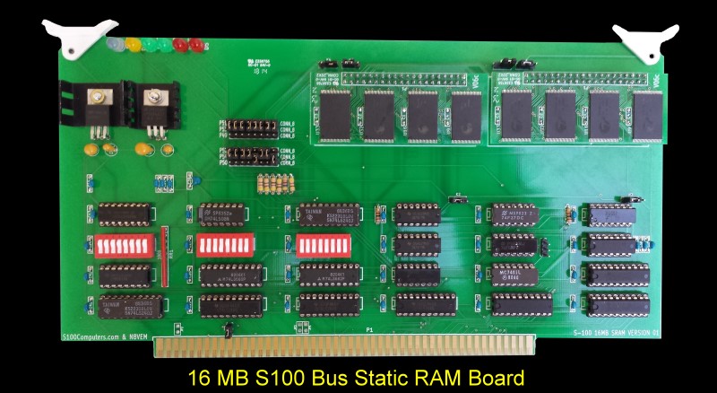
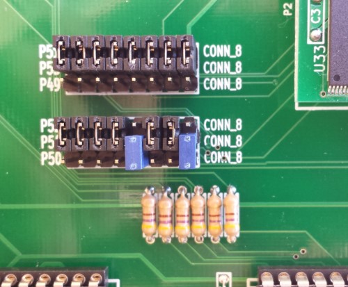
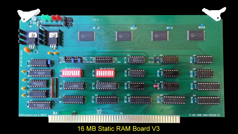
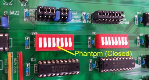
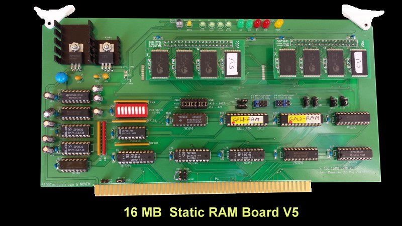
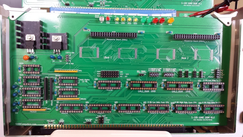
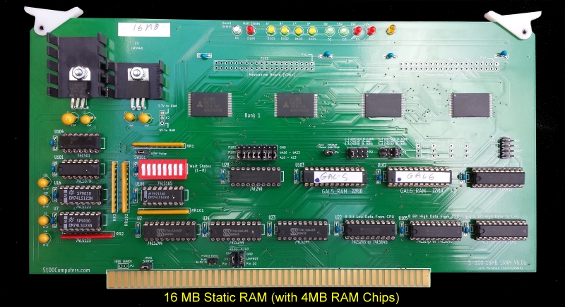
We will now build the board up in functional steps. Avoid the temptation of adding everything at once and popping it into your S-100 box. Step by step is faster in the end -- trust me.  However unlike our other CPU boards you have a chicken/egg situation here because you need a functional RAM board to test the board itself. The easiest approach is to start with an old S100 RAM board (of almost any kind) that is working.  Boot your system up with that board.  Insert all the IC's in our 16MG RAM except U19, U31 and U32.  Also bend out pin 4 of U10 (RDY).   Do not insert the two RAM mezzanine boards yet. Set all the dip switch positions of SW 2 to open (no wait states).  Set all switch positions of SW3 and SW4 to closed except SW4 position 5 (Phantom*).    Boot up your system and check that the Board Select LED D1 stays on all the time as you display memory 0 to FFFFH. check that pin 19 of U22 and U19 are pulsing low.

Next insert the remaining IC's including the two RAM mezzanine boards.  You must remove your old RAM board.   Your system should boot up.  If you have an 8086 board check the 1MG of RAM with memory moves etc.  If you have our 68K board do the same for the total 16MB of RAM. (The same test can be carried out with the 80286 board but you will have to program the monitor to work in protected mode, see here).

Please note: In an 
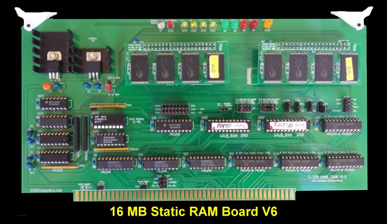
early version of the board there was an error in the jumpers for the mezzanine board. These mezzanine boards were labeled V02.  This mezzanine board has now been replaced by the V06c version.  But just in case you only have the V02 version see below.

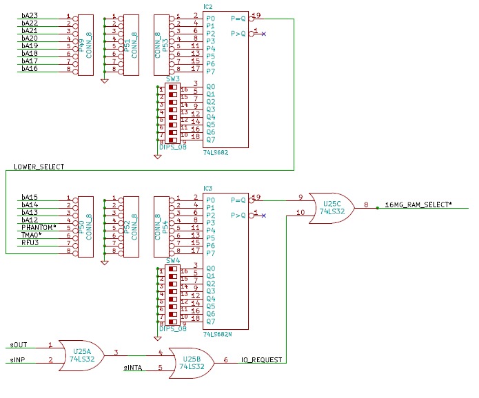
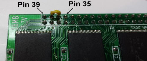
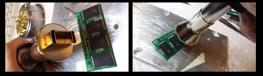
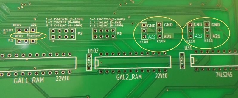
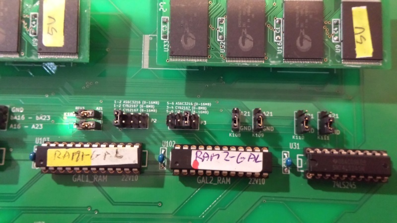
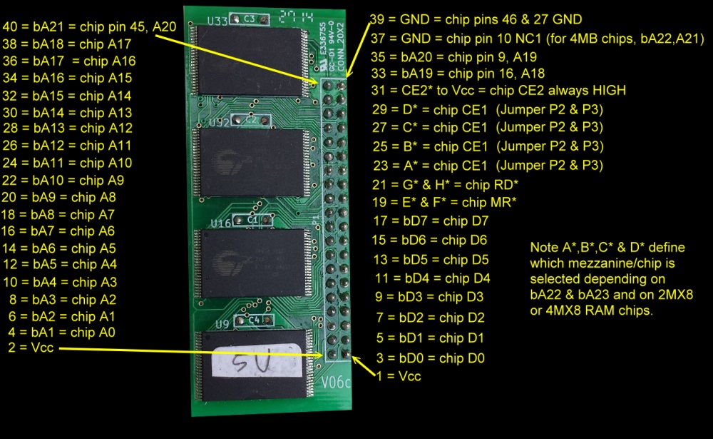
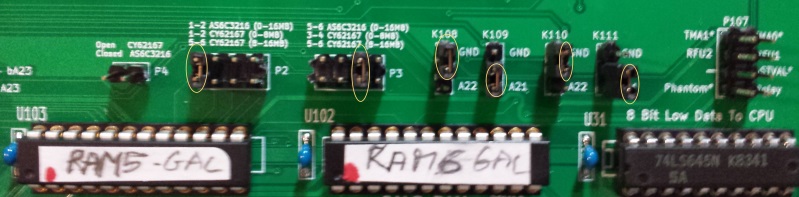
We drew up the schematic for these 16MB mezzanine boards when we were doing the early 32 MG RAM Board a 32 bit data bus board. For this reason the pin names do not really correspond to the actual address lines for this 8/16 bit bus board in the schematics included below.  Note this is just a labeling issue, (the RAM chips themselves could not care less), they only examine the 20 address lines coming into the chip.  However pin 17 of the RAM chip on the V02 mezzanine boards should be connected to address line bA20 from the parent board (mezzanine pin 37).  It is not.  This is easily corrected by jumpering pin 35 on the mezzanine board to its pin 37. See picture below. Jumpers K3 and K6 should not be connected to anything, jumpers K4 & K7 should be connected 2-3 (A21). This is not an issue for the V06c mezzanine boards.
   
  Mezzanine patch

David Fry has done an excellent write-up about this error and the corrections/options available for using either this above CY62167DV30 static RAM chips or the Alliance AS6C3216 static RAM chips.  He has gone on to explain how one can in fact use the newer AS6C3216 (4M X 8bit) static RAM chips using only two chips per mezzanine board.  Please see hereThanks David.  

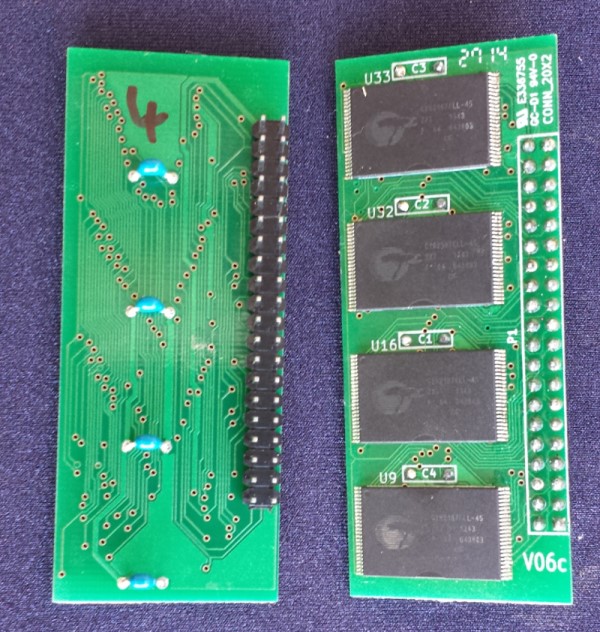
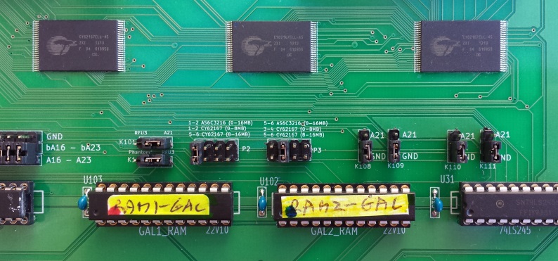
A corrected mezzanine board was later made and it is labeled V06c.  The chips I am using are the Cypress CY62167ELL-45ZXI 2MX8 Static RAM chips.  I obtained mine from Arrow Electronics, RENO, NV.   These are actually 5V chips but they also seem to run fine at 3.3V.

For these chips with 16MB of RAM the jumpers are:-

K4 & K7  2-3 (A21)
K3 & K6 1-2  (Ground)
K2 & K5  2-3  (Vcc)

JP8 Connected
K1 Unconnected


Here is a picture of the address line jumpers:-
     
 Address Jumpers
       
So far I have just tested this board with 8 bit read and writes on our Z80 and 6502 boards. I have also tested it with the Cromemco ZPU board and  Intersystem's II Z80 board. For 16 bit systems you will need a 16 bit CPU.  I have tested the board our own IEEE-696 compatible 8088, 8086 & 80286 boards. It appears to ran it fine with CPM86+ and MSDOS. The board also works fine with the 68000 CPU Board and an 80386 CPU S-100 board.  With the fast RAM access of these chips on this board no wait states are required.  

Bugs.
The only bug noted so far (apart from the above V02 mezzanine problem), is the RD/WR LEDs do not light up sufficiently. The pulses are too short. The next version of the board will use a 74LS123 will be used to stretch the pulses (see below).

A Second Prototype 16 MG Static RAM Board.
One thing that I did not like about the above 16MB static RAM board was the need for the two mezzanine boards.  While the board works absolutely fine with any CPU I used with it (even our 80386 CPU board) it is a tight fit in the S100 box. Also dare I say it does not look pretty!  Putting 8 CY62167DV30 static RAM chips directly on an S100 board would be both difficult to fit and risky in terms of SMD soldering for many users.   With the advent of the newer AS6C3216 (4M X 8bit) static RAM chips, soldering 4 chips on a board becomes more practical.  

So I rearranged the board so it can be configured as a S100 bus 8MB board using the CY62167 chips or 16MB using the AS6C3216 chips.   We will call this board the
16MB Static RAM V3 board, (there was an early V2 prototype). While the 74LSxx chips have changed little from the mezzanine board, the top half of the board had to be completely re-routed to accommodate the 4 SMD chips.  Here is a picture of the board:-
 
  16MB Static RAM V3

I would like to stress that the main reason for this board is cosmetic. The above mezzanine board works perfectly fine.  This board is just cleaner and if you go for the AS6C3216 (4M X 8bit) static RAM chips, more expensive.  BTW, I have not actually tried these chips on this prototype board -- because they are currently expensive. I will do so on the final production board of course.

Removing SMD RAM chips from mezzanine boards.
Much to my surprise (and delight), it turns out it is easy to remove the above SMD CY62167DV30 static RAM static RAM chips from the mezzanine boards and reuse them on this board.  The trick is to use a specialized hot air adaptor that heats only the RAM pins and not the chip itself.   I use a Aoyue 968A soldering station that has a built in hot air blower. I set the temperature to 400 degrees.  The unit did not come with a 48 pin TSOP adaptor (it had many others). I obtained it on eBay, they are common.  Hold the heat gun vertically over the chip, heat for a few seconds and with a blade raise the chip. I immediately move the chip to a flat metal plate to quickly cool it. Here is a picture of the setup.
    
  Removing RAM


A Production S-100 Board.

The above board work fine with all S100 bus CPU's I used it for.  I proceeded to have a production board made (by PCBCart).  The only minor change was a repositioning of the 5V regulator heat sink such that a larger one could be used.   Actually it turns out that because there are so few chips on this board a larger heat sink was not really necessary.

Assembly of the board follows the standard procedures we used in the past.  Because this board resides in RAM starting at 0H, if it's the only RAM board in your system, it will hang if the board is no working correctly.   Its best to first assemble the board without the RAM chips and the data bus drivers U19, U31 and U22 and see if the LED flash correctly with 8 or 16 bit RAM reads using another RAM board.  The Board Select LED, D1, should stay on all the time.

If the board is used as an 8MB RAM board (using four 2MX8 RAM chips) ,  Jumper P2 1-2 and P3 3-4.  Jumper K3 2-3.  Jumper JP8.  Be sure to set the RAM voltage correctly to 5V or 3.3V with jumper K2. 
 
If the board is used as an 16MB RAM board (using four 4MX8 RAM chips) ,  Jumper P2 1-2 and P3 5-6.  Jumper K3 1-2.  Jumper JP8.  Be sure to set the RAM voltage correctly to 3.3V.    It is probably safer to solder a wire for jumper K2. Once the RAM chips are soldered into place that  voltage setting jumper should never change.  If you have the 80386 CPU board you can test all 16MB of RAM using the 80386 monitor (in protect mode) RAM test.  You can use the memory map and move memory commands as a crude RAM test with the 68K CPU board.
 
Here is a picture of the final board:-
Bank 1 will normally address RAM from 0H to 3FFFFF (or 7FFFFF). Try these two chips first to be sure your soldering techniques are OK.
   
  16 MB RAM V3

The normal switch settings are all switches closed except the phantom line.  See here:-
   
  Phantom Line


A Third Prototype 16 MG Static RAM Board.
One final thing that I did not like about the above 16MB static RAM boards was the breakout of the 8/16 bit data bus IEEE-696 conversion using 74LSxx chips.  While the circuit got the job done fine, there is overhead in the RAM access time.  With static chips like these clearly not an issue for an 8080. However I want to use these RAM boards with chips like the 80386 and 80486 at 10+MHz on the bus.  One or two GAL's clearly fit the bill for a board like this.  I realize people may have become jaded with yet another S100 bus RAM board, so I have tried here to insure this would be the last RAM board we would ever need!  I have taken the above V3 board and added the following extras (see below). I calling this the
V5 static RAM board.  (There was a V4 along the way).  This board has the following additional features:-
  1. I did not want to change the basic RAM board circuit. It has proven itself time and again to be very reliable with any CPU board I could throw at it. Common easy to obtain 74LSxx chips are used throughout.

  2.  I wanted to hand lay down broad power traces to all the boards IC’s for more even power distribution.

  3. I have inserted a trace “Keep out Area” on the front of the board so there is no danger of the 5V and 3.3V regulator heat sinks touching a critical trace beneath.

  4.  I added two 22V10 GALs to replace a number of 74LSxx chips.  This greatly simplifies the board and somewhat speeds up the RAM access times.  I realize not everybody is familiar with GAL’s. Please see here for more information about GALs. For those people and beginners I will supply the pre-programmed Lattice 22V10 GALs. The PALASM code is shown below.  Again these GAL’s are fairly common (Jameco #39159 for the 15ns variety).  

  5.  I have added a wait state circuit (0 - 8 RAM Rd/Wr wait states) to accommodate very fast S100 boards such as our 80386 and 80486 boards.

  6.  People should be able to simply switch IC’s from the old board to this new one. Two new GAL ICs is the only major change. 

  7. While the board is really built to meet the 16MB addressing range of the IEEE-696 bus, I have added jumper options so the board can be used in older systems like an Altair or IMSAI which only use a 16 bit address bus.  Altair/IMASAI RAM write protect/unprotect can also be implemented on this board.

  8. The board can accommodate EITHER the dual Mezzanine RAM boards described above (V6.0c),  for 16MB of static RAM, or 8MB by soldering the 4 SMD  CY62167DV30 static RAM chips directly on the board, or 16M by soldering 4 of the newer SMD  AS6C3216 (4M X 8bit) static RAM chips on the board.

  9.  Last but least, I relabeled much of the Silk Screen to be more relevant. For example placing IC numbers above their pin locations etc.   

The main difference with this board is the use of the two 22V10 GALs for 8/16 bit data bus decoding. 
First lets look at GAL1.  The main function of this GAL is to decode the boards 8 and 16 bit RAM Read and Write signals.
Here is the GAL22V10 relevant code:-

Pin 1  bpSYNC
Pin 2  bpDBIN
PIN 3  bsXTRQ                    ;Active Low
PIN 4  bpWR                      ;Active Low
PIN 5  bsMEMR                    ;Active High
PIN 6  bA23
PIN 7  bA22
PIN 8  MemChip                   ;2MB or 4MB ram chips (Note error in board layout)
                                 ;K101 pin 1 should be tied to high, pin 3 to ground.
                                 ;For CY62167 2MG RAM chips, leave K101 unconnected (will read as high).
                                 ;For AS6C3216 4MG RAM chips, jumper K101 pin 2 to ground
PIN 9  sINTA
PIN 10 sINP
PIN 11 sOUT
PIN 13 PHANTOM                   ;Input, for RAM access this signal must be high. (Is Low to disable a RAM window)

;----- OUTPUT SIGNALS --------

PIN 14 D                         ;Active low
PIN 15 C                         ;Active low
PIN 16 B                         ;Active low
PIN 17 A                         ;Active low
PIN 18 bsMEMR@                   ;Inverted bsMEMR for bus drivers U19, U31, and U22
PIN 19 BOARD_SELECT              ;Active HIGH if board is selected
PIN 20 WR16
PIN 21 WR8
PIN 22 RD16
PIN 23 RD8

;--------------- Boolean Equation Segment ------

EQUATIONS

/BOARD_SELECT = sINTA + sINP + sOUT + /PHANTOM      ;LOW to inactivate board if INTA,Port IN/OUT or PHANTOM*


RD8 = bpDBIN * bsXTRQ * BOARD_SELECT   *  /bpSYNC    ;bsXTRQ will be HIGH if 8 bit data

RD16 = bpDBIN * /bsXTRQ * BOARD_SELECT *  /bpSYNC    ;bsXTRQ will be LOW if 16 bit data

WR8 = /bpWR * bsXTRQ * BOARD_SELECT       *  /bpSYNC 

WR16 = /bpWR * /bsXTRQ * BOARD_SELECT  *  /bpSYNC 


bsMEMR@ = /bsMEMR                                   ;Inverted MEMR for bus drivers U19, U31, & U22

/A = /bA23 * /bA22 * BOARD_SELECT                   ;Ignore the possibility of 4X 4MB chips on board
                                                    ;for now with this GAL code. (see above if required).
/B = /bA23 * bA22 * BOARD_SELECT

/C = bA23 * /bA22 * BOARD_SELECT

/D = bA23 * bA22 * BOARD_SELECT


Clearly quick and simple code.  BTW, I know some people like to predefine the active state of a pin the definition section. I find it clearer to do so in the equations.

GAL2 is a bit more complicated.  It is provides the enable signals for the bus drivers and the actual RAM chips.  The code could actually be simplified by using multiple brackets within the equations, but PALSAM complains. You need to use the optimization switch/option.  GAL code space is not a problem here!
Here is the GAL22V10 relevant code:-

Pin 1  pSYNC
Pin 2  RD8
PIN 3  RD16
PIN 4  WR8
PIN 5  WR16
PIN 6  bA0
PIN 7  BOARD_SEL
PIN 8  sXTRQ
PIN 9  NC
PIN 10 NC
PIN 11 PROTECT                        ;Old S100 bus signal. Active HIGH
PIN 13 UNPROTECT                      ;Old S100 bus signal. Active HIGH

;----- OUTPUT SIGNALS --------

PIN 14 X
PIN 15 SIXTN
PIN 16 Z
PIN 17 Y
PIN 18 E
PIN 19 F
PIN 20 G
PIN 21 H
PIN 22 PROTECT_LED                     ;Old S100 bus signal (PROTECT STATUS). Active HIGH
PIN 23 PHANTOM                         ;For RAM access this signal must be high. (Active Low to disable a RAM window)


;------------------ Boolean Equation Segment ------

EQUATIONS

/X = RD8   * /PROTECT   * PHANTOM
   + RD16  * /PROTECT   * PHANTOM
   + WR16  * /PROTECT   * PHANTOM
   + RD8   * UNPROTECT  * PHANTOM
   + RD16  * UNPROTECT  * PHANTOM
   + WR16  * UNPROTECT  * PHANTOM

/SIXTN = sXTRQ * BOARD_SEL * /PROTECT   * PHANTOM
       + sXTRQ * BOARD_SEL * UNPROTECT  * PHANTOM


/Z = RD16 * /PROTECT  * PHANTOM
   + WR16 * /PROTECT * PHANTOM
   + WR8  * /PROTECT  * PHANTOM
   + RD16 *  UNPROTECT * PHANTOM
   + WR16 *  UNPROTECT * PHANTOM
   + WR8  *  UNPROTECT * PHANTOM

/Y = RD8 * /bA0 * /PROTECT * PHANTOM
   + WR8 *  bA0 * /PROTECT * PHANTOM
   + RD8 * /bA0 *  UNPROTECT * PHANTOM
   + WR8 *  bA0 *  UNPROTECT * PHANTOM

/E = RD8  * bA0 * /PROTECT * PHANTOM
   + RD16       * /PROTECT * PHANTOM
   + RD8  * bA0 *  UNPROTECT * PHANTOM
   + RD16       * UNPROTECT * PHANTOM


/F = RD8  * /bA0 * /PROTECT * PHANTOM
   + RD16        * /PROTECT * PHANTOM
   + RD8  * /bA0 * UNPROTECT * PHANTOM
   + RD16        * UNPROTECT * PHANTOM


/G = bA0  * WR8 * /PROTECT * PHANTOM
   + WR16       * /PROTECT * PHANTOM
   + bA0  * WR8 *  UNPROTECT * PHANTOM
   + WR16       *  UNPROTECT * PHANTOM


/H = /bA0 * WR8 * /PROTECT * PHANTOM
   + WR16       * /PROTECT * PHANTOM
   + /bA0 * WR8 *  UNPROTECT * PHANTOM
   + WR16       *  UNPROTECT * PHANTOM

/PROTECT_LED = PROTECT                ;Signal directly to LED and if jumpered
                                      ;S100 bus OC signal 69

Here are two pictures of the board.  The first is the board using two of our Mezzanine boards.
The second is the board using 4 SMD RAM chips directly on the board.
Obviously when you solder in the SMD chips you cannot use the mezzanine boards.

  Prototype Board1
   
  Prototype Board 2

I would like to stress that the main reason for this board is cosmetic. The original mezzanine board or V3 boards work perfectly fine.  This board is just cleaner particularly if you go for the AS6C3216 (4M X 8bit) static RAM chips,  They are however currently much more expensive.  

There are 6 silkscreen errors on the board for the labeling of the jumpers K108, K109, K110 and K111 and K1.
They should have been labeled as shown here (in yellow):-
 
  V5 jumpers 1
   

A typical jumper arrangement of 16MB (using two V06c mezzanine boards would be as shown here:-
   
  V5 Jumpers 2


All P105 jumper pins to all p101 pins
K101 1-2.
K1  1-2  (Phantom*)
P2 1-2
P3  5-6
K108 2-3
K109 2-3
K110 2-3
K111 2-3

JP101 jumpered for SIXTN*
For most CPU's 0 Wait states are required so all the switches of SW101 are open.

Be sure you have the correct 3.3 or 5.0 volts, (jumper K2), to your RAM chips.

For the situation where
we solder 4 SMD  CY62167DV30 static RAM chips directly on the board the jumper arrangement is the same except for P3 is now 3-4. Here is a picture. Remember the silkscreen labels are wrong (see above).
    
  Jumpers 3

Pin labels on the V06c Mezzanine boards

In retrospect I should have labeled these mezzanine boards completely different. They were first used for the 32MB 80386 board (4 of them).  To add flexibility for these expensive chips I re-used them here on these 16MB boards.  This has led to confusion terminology for the pins.  For example, pin 37 on the V06c Mezzanine boards  goes to pin 10 on the RAM chips.   This is A21 on the 4MX8 chips, NC on the 2MX8 chips.  Pin 40  on the Mezzanine board goes to pin 45 on the chips this is A20 on the chips (4M & 2M chips).  To make things even more confusing remember we are talking 16 bit access -- there is no bA0, so the actual chip address names are +1, For example chip A0 = actual bA1, chip A1 = bA2....... chip A21= bA22. Here is a diagram which I hope helps explain the pinouts better:-


  Chip Pinouts

BUGS
Apart from the silkscreen labeling error described above,
I have noticed one other small bug on this board so far.  The GAL1 chip (U103) needs to know if we are using 2 or 4MB RAM chips on the board.   Pin 8 of U103 in the GAL software uses a high/low pin 8 input to determine this.  Unfortunately the input on the actual board (K101) does not feed this to that pin.    Most people will be using the 2MB RAM chips (4) on their mezzanine boards (or the chips soldered directly to the board), so if you don't jumper K101,  pin 8 will read high.   If instead you have two 4MB RAM chips on your mezzanine boards (or have four 4MB chips soldered directly to the board), you need to jumper pin 2 of K101 to ground.  Alternatively you can adjust the actual GAL code itself as I did (see above).   

There is a subtle error with the S100 bus SIXTN* output from GAL2 (U102,pin 15 , via JP 101). This signal is low to let a CPU know the board is capable of 16 bit transfers.  The IEEE-696 specs specify it as OC format.  The output from GAL2 is a normal TTL format.   This is normally not a problem with all our 16 bit CPU boards -- they assume 16 bit data transfers and so don't actually use the signal.  If this were the only RAM board in the system it would be even less of a problem, but our MSDOS Support board with its onboard ROMs also lowers SIXTN* when accessed.  Under such conditions this 16MB RAM board would not be selected and so its TTL level SIXTN* would go high.  We have a conflict with the two gates.

The easiest solution is not to activate SIXTN* on this board (remove the JP 101 jumper).  This will not affect any of our current CPU's.  However it will be a problem with the upcoming 80486 board which actually can handle 16 bit data in 8+8 byte chunks IF SIXTN* is not low.  As a patch you can use the unused OC 74LS01 (U105) gate pins 13, 12, 11 as a buffer. Connect JP101 pin 1 to pins 11 & 12 of U105. Connect its pin 13 to to JP101 pin 2.  The output from GAL_RAM2 pin 15 will now need to be inverted.  So use:-

SIXTN = sXTRQ * BOARD_SEL * /PROTECT * PHANTOM * /pSYNC    ;Do not use /SIXTN
       + sXTRQ * BOARD_SEL * UNPROTECT * PHANTOM * /pSYNC


This error is corrected on the V6.0 board.  It is also not a problem on the earlier/above non GAL based 16K Boards boards.

Recently I have noticed that the buffers U19, U31 and U22 (in particular U19) are sensitive to the 74LS245 manufacturer.  With Ti chips I found that booting MSDOS with even our old 8086 board  sometimes hang.  At first I thought it was a bad batch of chips. But two different/dated batches of Ti chips caused the same problem. Signetics chips and some others seemed to work OK.  Using 74F245 chips always failed. The good news is using any type of the newer 74LS645 chips always worked fine.    This is a bit unnerving as it indicates a timing problem with the circuit.   I now realize that since we are using GAL's a much better circuit 8/16 bit routing circuit can be done with 4 buffers rather than the High/Low byte shifting 3 buffer arrangement on these boards (See below). 

Note if you solder the RAM chips directly to the board. Instead of 4 chips you can just solder 2 chips into "Bank 1"  (the two left most chips). This will give you a fully functional 4MB Board.


A Fourth 16 MG Static RAM Board.
Apart from the above silkscreen errors on the V5 board, one thing that I did not like about all the above 16MB static RAM boards was the way 8 and 16 bit data was passed data to/from the S100 bus.  In all the previous  boards the 8 and 16 bit data travels to/from the S100 bus via  three 74LS245's.  This was to  simplify the TTL logic circuit for the data paths.  With the use of a GAL we can now have more direct/faster  paths.  These can be represented as follows:-
  
  Old Data Buffers 
   
  New Data Buffers

To make sense of the above layout, is very important to understand how 16 bit CPU's send 8 bit data.  For example for an Intel 8086, if it is sending out an 8 bit byte; If it is to an even/low address in RAM it will be on the lower half of its 16 bit data path.  If it is to an odd/high address  in RAM it will be on the upper 8 bits of its data path.  Since the S100 bus has a seperate read and write 8 bit data bus, the upper and lower 8 bits have to be shifted depending on if its a read/write and odd/even address.  Of course 16 bit data go straight across.

Also now with the low chip density on the board, it is not only possible to allow the use of the two Mezzanine boards, or solder four SMD chips directly to the board, we can use wide signal traces for the critical S100 bus lines.  The above errors on the V5 board were corrected. Finally the board was (one more time) polished, with more silk screen labels and information.  The board seems to work with all our S100Computers CPU boards as well as those of the late 1960's and 1970's.  This board will be called the V6 16MB Static RAM Board.

Step By Step Building the V6 16MB Static RAM Board
The steps required to build this board are essentially the same as for the previous boards in this series.
Solder in all the required IC sockets, resistors, resistor arrays, capacitors, jumpers, 8 pin dip switch, LEDs, and the two voltage regulators.  Be sure you put the resistor array in with the correct orientation of pin 1. Check their values before  soldering (they are difficult to remove).   Also be sure you solder the LED's in correctly. Normally the longest lead goes to the square pad on the board.
 
For prototype boards I generally use "double swipe" IC sockets. For a critical board like this I prefer to use "Machine Tooled" IC sockets.  However they are more expensive and you have to be particularly careful not to bend the IC pins. 

Check the voltage to sockets on the board is above 5V by placing the board in your S-100 system using an extender board. With no load you will typically get 5.00V  (+/- 0.25V).  BTW, your system should boot and run correctly with its Z80 master CPU board. If not, you have a serious solder bridge somewhere on the board.  Before you do anything else with a magnifying glass go over every socket on the board and examine for a proper solder joint. I like to "reheat" each joint just to be on the safe side. The silk screen/varnish on these boards us quite thick. It's easy not to have a good solder joint for the ground pins.  Double check.   Extra time here will save you hours later.  Pin 1 of K2 should read 3.3 Volts.
here is a picture of the board at this stage:-
   
  V6 Bare Board
    
Next program the two GAL's (RAM5_GAL and RAM6_GAL).  The files are available at the bottom of this page.  The key code is as follows:-

RAM5_GAL:-
/BOARD_SELECT = sINTA + sINP + sOUT + /PHANTOM@  * /bpSYNC        ;LOW to INACTIVATE the board


/RD8@         = bpDBIN * bsXTRQ@ * BOARD_SELECT   * /bpSYNC       ;bsXTRQ will be HIGH if 8 bit data

/RD16@        = bpDBIN * /bsXTRQ@ * BOARD_SELECT  * /bpSYNC       ;bsXTRQ will be LOW if 16 bit data

/WR8@         = /bpWR@ * bsXTRQ@  * BOARD_SELECT  * /bpSYNC

/WR16@        = /bpWR@ * /bsXTRQ@ * BOARD_SELECT  * /bpSYNC

bsMEMR@       = /bsMEMR                                           ;Inverted MEMR for U19, U31,& U22


/A            = /bA23 * /bA22 * BOARD_SELECT  * ChipType          ;If 2MB RAM chips
            +   /bA23 * BOARD_SELECT  * /ChipType                 ;If 4MB RAM chips

/B            = /bA23 * bA22 * BOARD_SELECT   * ChipType

/C            = bA23 * /bA22 * BOARD_SELECT   * ChipType
            +   bA23 * BOARD_SELECT   * /ChipType

/D            = bA23 * bA22 * BOARD_SELECT    * ChipType


RAM6_GAL:-

/S100_8_RD_OE@   = /RD8@ * bA0 * /pSYNC                  ;U19, 8 Bits to CPU, odd/high address
                +  /RD16@ * /pSYNC                       ;Any 16 bit data Read
                +  /WR16@ * /pSYNC                       ;Any 16 bit data Write

/S100_8X_RD_OE@   = /RD8@ * /bA0 * /pSYNC                ;U31, 8 Bits to CPU even/low address

/S100_8_WR_OE@   = /WR8@ * /bA0 * /pSYNC                 ;U22, 8 Bits from CPU even/low address
                +  /RD16@ * /pSYNC                       ;Any 16 bit data Read
                +  /WR16@ * /pSYNC                       ;Any 16 bit data Write

/S100_8X_WR_OE@   = /WR8@ * bA0 * /pSYNC                 ;U105, 8 Bits from CPU odd/high address

/SIXTN@ = /sXTRQ@ * BOARD_SEL * /pSYNC                   ;Acknowledge we can do 16 bit data transfers


/E = /RD8@ * bA0  * BOARD_SELECT
   + /RD16@       * BOARD_SELECT

/F = /RD8@ * /bA0 * BOARD_SELECT
   + /RD16@       * BOARD_SELECT

/G = /WR8@ * bA0  * BOARD_SELECT
   + /WR16@       * BOARD_SELECT

/H = /WR8@ * /bA0 * BOARD_SELECT
   + /WR16@       * BOARD_SELECT

PROTECT_LED = /PROTECT                                 ;Signal directly to Protect LED, (High/off)

With both these GALS in place add the following IC's.
U104,U16,U101 and U7.
Add U2, U24, and U23.
For systems that utilize all 24 address lines, connect all jumpers on P105 to P101.
Add U28
Add U106 and jumper JP101. Jumper K102 and K103 1-2.
Normally no wait states will be required with this board so make sure all switches in SW101 are open
Insert the board in your system using an older RAM board.  The Z80 should boot up.  If not backtrack by removing IC's to locate the problem.
The "8R" (D2) should be lit as well as the Board Select (D1) LED.  Fill RAM wit a value should light up the "8W" (D3 ) LED.  Only the "A*" D101 LED should be on.  Note U22,U105, U 19 and U31 are not yet installed.

Even if you are going to solder the RAM chips directly to the board, it's best to initially use the mezzanine boards . Carefully install both.  Be particularly careful to set the correct RAM voltage using the jumper K2 (3.3 volts, 1-2. Or 5 volts, 2-3).

For 2MB RAM chips (CY62167DV30 static RAM )  jumper P2 1-2,  P3 5-6, K108 1-2, K109 2-3, K110 1-2 and K111 2-3.
There are no jumpers needed for P107.  Here is a close-up picture of these jumpers.
   
    
  V6 Jumpers
   

Insert the board in your system, and repeat the above test.

Next remove all other RAM boards you have in your system. 
Insert the data buffers U19, U22, U31 and U105.  best to use 74LS645's but 74LS245's are fine for all but the fastest CPU's.

Boot up your system. If the monitor does not sign on you have a RAM access problem.  To debug remove the four above buffers, insert another working RAM board and run RAM read write diagnostic tests looking for where a signal is not correct.  I have included below an 8 bit only version of the RAM6_GAL to help in debugging -- using only U19 and U22.  This will not work with 16 bit CPU's.

If you have one of the S100Computers 8086 etc. CPU's (or the 68K CPU) you can checkout RAM above 64K.  MSDOS should boot with this board with no problems.

If you have the S100Computers 80386  board you can run an extensive RAM test of the whole 16MB or RAM using the monitor "J" command.
Here is the finished board:-
    
V6 Board

Note if you solder 4 of the RAM chips directly to the board you will have a very nice "clean" 8MB Board.   Here is a picture:-    
   
  V6 Board-2


You can just solder 2 chips into "Bank 1"  (the two left most chips). This will give you a fully functional 4MB Board. 
If you solder in directly 4 of the  AS6C3216 (4M X 8bit) static RAM chips you will have a 16MB RAM board.  Here is a picture of such a board:-
     
  V6 with 16MB RAM
  
These (4MB X 8) chips were from Digi-Key (#1450-1026-ND) at $12 each they are not cheap,  but I remember the days when a 16K RAM S100 board cost $400.  If you use this arrangement be sure to permanently jumper K2 to 3 Volts. 5 Volts even briefly, will toast these RAM chips.

Notes
Dave Rataj pointed out that with the Compupro CPU286 board the GAL equation for the SIXTN line which is qualified with pSync, delays the acknowledge just past the rising edge of the T1 click (which the CPU uses to determine if a transfer can take place). The CPU286 Compupro board was initiating a 2 byte transfer even though the 16MB memory was asserting the SIXTN. Removing the pSync from the GAL equation fixes this problem and the board works fine in 16 bit mode.

Henry Broekhuyse noted that using his logic analyzer, that the 4MB & 16MB RAM boards got along okay with his Compupro 80286 processor S100 board but were unable to reliably keep up with the speed at which the hard drive DMA controller was trying to bring data into RAM during the boot process. Adding wait states did not help, which suggests to him there is an internal timing problem with these boards that becomes an issue at high speeds.

Along the way he also discovered that this board is significantly more reliable when only partially populated with RAM chips. He did a lot of swapping of RAM chips and their locations to confirm this wasn’t related to one or more faulty RAM chips and/or sockets and/or soldered connections. One factor that got both boards to work was the replacement of all “LS” parts with their “F” speed equivalent, when available. He noted he also ran into the same problem I commented on in the build of the 16MB board with respect to the data bus transceivers – on the 4MB board 74F245s always fail, and only select 74LS245s work. He is awaiting delivery of some 74LS645s to test them out with this board.


A Production Board
Realizing that a number of people might want to utilize a board like this together a group of people on the Google Groups S100Computers forum
"group purchases" are made from time to time. Please see here for more information.

Also please see here for more information about the above mezzanine boards. 

The links below will contain the most recent schematic of this board.
Note, it may change over time and some IC part or pin numbers may not correlate exactly with the text in the article above.


MOST CURRENT 16MB V1 STATIC  BOARD SCHEMATIC    (V1, Production board 5/28/2014)
MOST CURRENT 16MB V1 STATIC  BOARD LAYOUT   (V1, Production board 5/28/2014)
Most current KiCAD files for this V1 board  (S100 16MB SRAM-001 (1).zip 11/5/2014)

OLD 8MB MEZZANINE BOARD (V02) SCHEMATIC    (V1, Production board 4/21/2014)

MOST CURRENT 8MB MEZZANINE BOARD (V06c) SCHEMATIC    (V6c, Production board 4/21/2014)
MOST CURRENT 8MB MEZZANINE BOARD (V06c) LAYOUT    (V6c, Production board 4/21/2014)


MOST CURRENT  V2 - 16MB STATIC  BOARD SCHEMATIC    (V1, Prototype board 10/29/2014)
MOST CURRENT  V2 - 16MB STATIC  BOARD LAYOUT  (V1, Prototype  board 10/29/2014)
Most current KiCAD files for this board  (S100 16MB SRAM- V3).zip  11/5/2014)

MOST CURRENT  V5 - 16MB STATIC  BOARD SCHEMATIC    (V5, FINAL 11/3/2015)
MOST CURRENT  V5 - 16MB STATIC  BOARD LAYOUT       
(V5, FINAL 11/3/2015)
Most current KiCAD files for this board                                                     (V5, FINAL 11/3/2015)
MOST CURRENT  V5 GAL Files                                     (V5, Corrected 9/10/2016)
BOM List for V5 Board                                                       
(V5, Final 11/3/2015)


MOST CURRENT  V6.0a - 16MB STATIC  BOARD SCHEMATIC   
(V6.0a, Final 12/15/2015)
MOST CURRENT  V6.0a- 16MB STATIC  BOARD LAYOUT    (V6.0a, Final 12/15/2015)
Most current KiCAD files for this V6.0a board    (V6.0a, Final 12/15/2015)
V6d Mezzanine KiCAD files    (V06d, Final 4/1/2017)
MOST CURRENT  V6.0a GAL Files    ((V6.0a, Final 12/15/2015)
BOM for 16MB RAM Board  (From Richard Pope  11/10/2017)
BOM for V0.6 16MB RAM Board  (From Henry Broekhuyse 9/20/2020)


Other pages describing my S-100 hardware and software.
Please click here to continue...


This page was last modified on 02/21/2021